
High-Speed Carrier Transport and Tunneling Devices
High-speed semiconductor devices operate on time scales where carrier transit dynamics become the primary limiting factor. Two broad mechanisms dominate:
- Drift/Diffusion Transport → Carriers accelerate under an electric field, limited by scattering and velocity saturation.
- Quantum Tunneling → Carriers penetrate through potential barriers in sub-picosecond times, largely independent of scattering.
In addition, special devices such as the Esaki (tunnel) diode exploit tunneling to achieve negative differential resistance, while IMPATT diodes use avalanche multiplication combined with drift-region delay to generate microwave oscillations.
Drift/Diffusion Transit Time
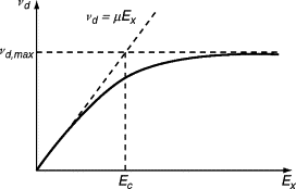
For a uniformly doped semiconductor slab of length L subjected to an electric field E, the carrier drift velocity is:
where μ is the carrier mobility.
At high fields, velocity saturates at , giving:
The mean drift transit time is then:
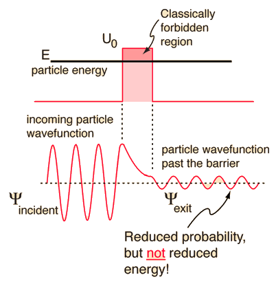
Quantum Tunneling Transit Time
For a barrier of width W and height , the WKB approximation gives the transmission probability:
where is the effective mass and E the carrier energy.
The effective tunneling transit time is often estimated as:
where ΔE is the energy uncertainty associated with the tunneling process.
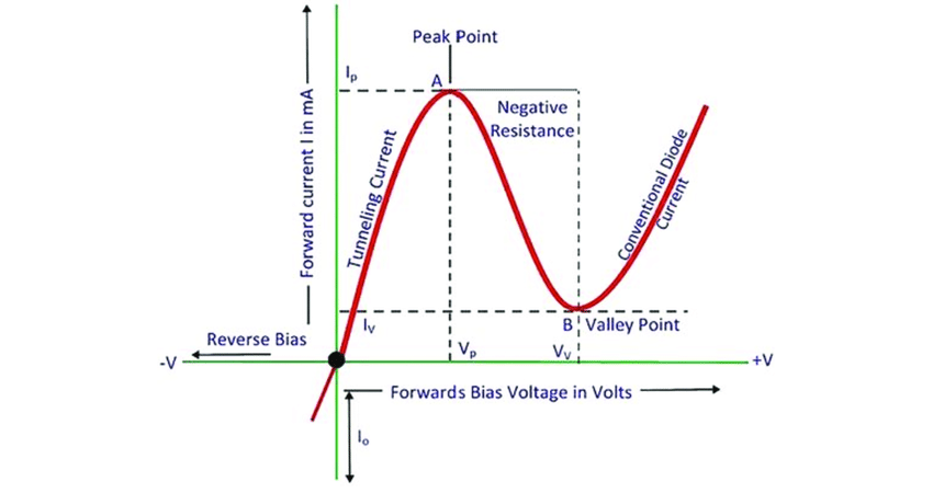
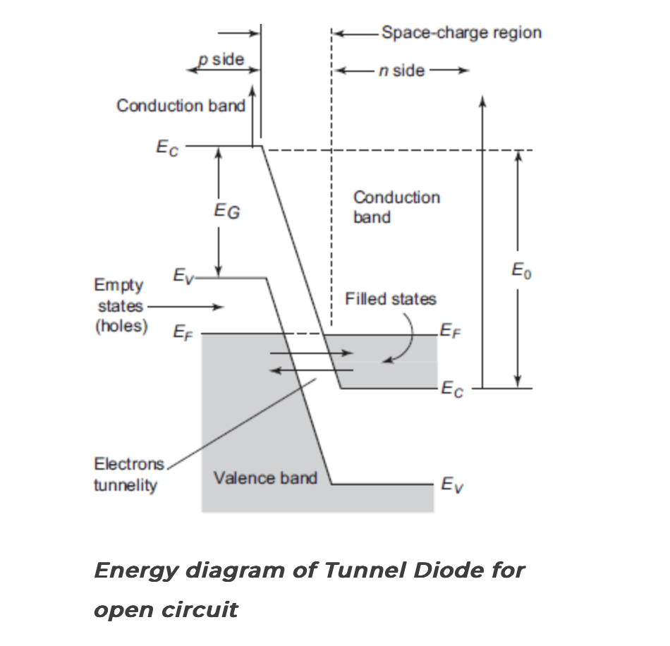
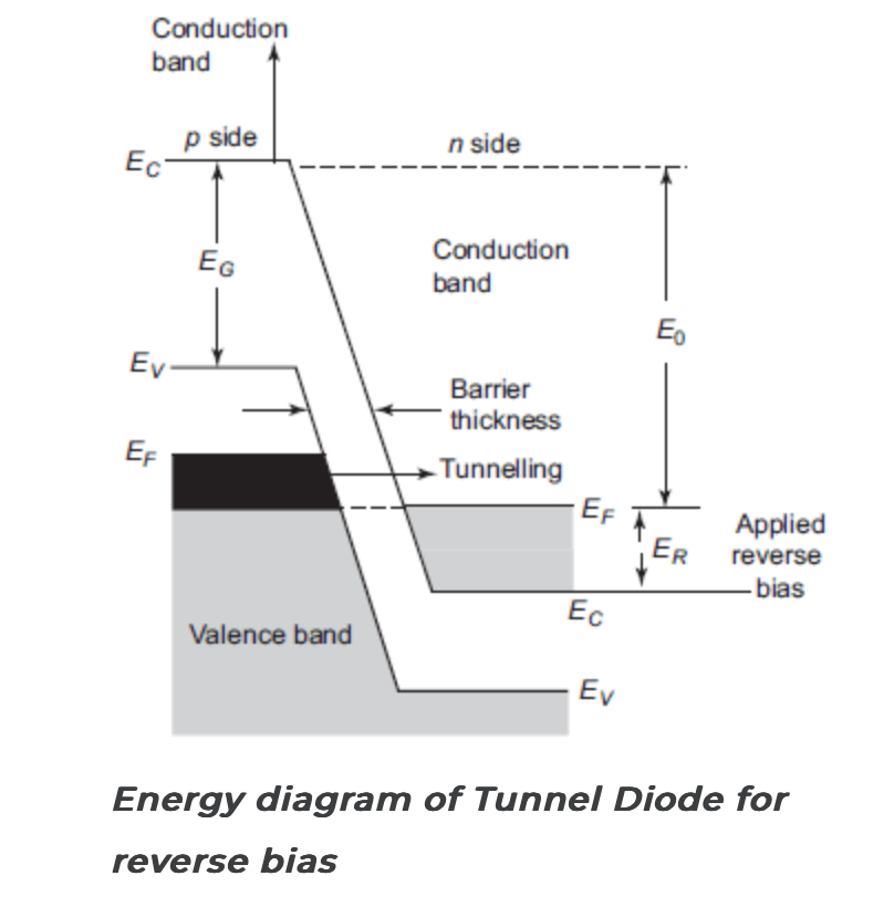
Esaki (Tunnel) Diode Theory
A tunnel diode consists of a heavily doped p⁺n⁺ junction with a
depletion width ≈ 10 nm.
Its I--V characteristic is dominated by interband tunneling:
- Low forward bias → Filled conduction-band states on the n-side align with empty valence-band states on the p-side, enabling tunneling and producing a current peak at .
- Moderate bias → The overlap decreases, reducing current (negative resistance region).
- High bias → Normal diffusion current dominates again.
The Peak-to-Valley Current Ratio (PVCR) is:
where is the peak current and the valley current.
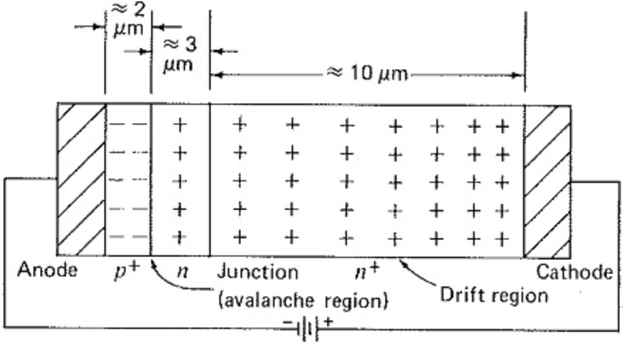
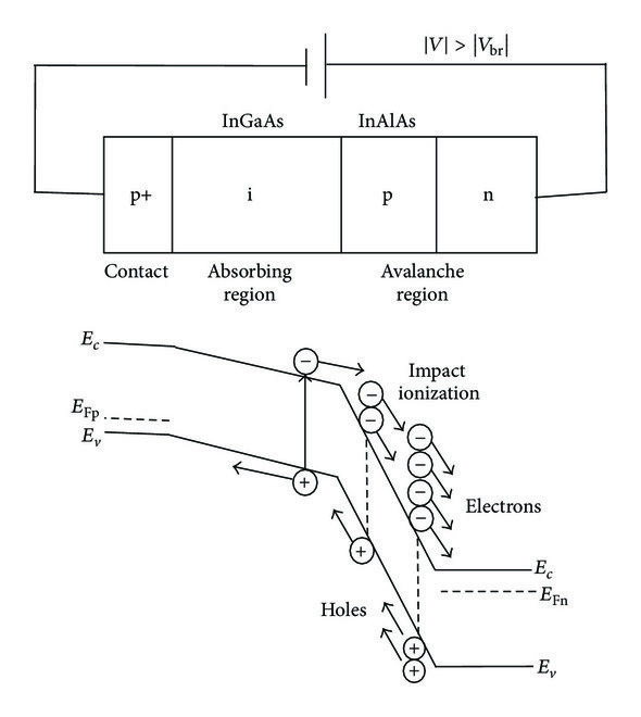
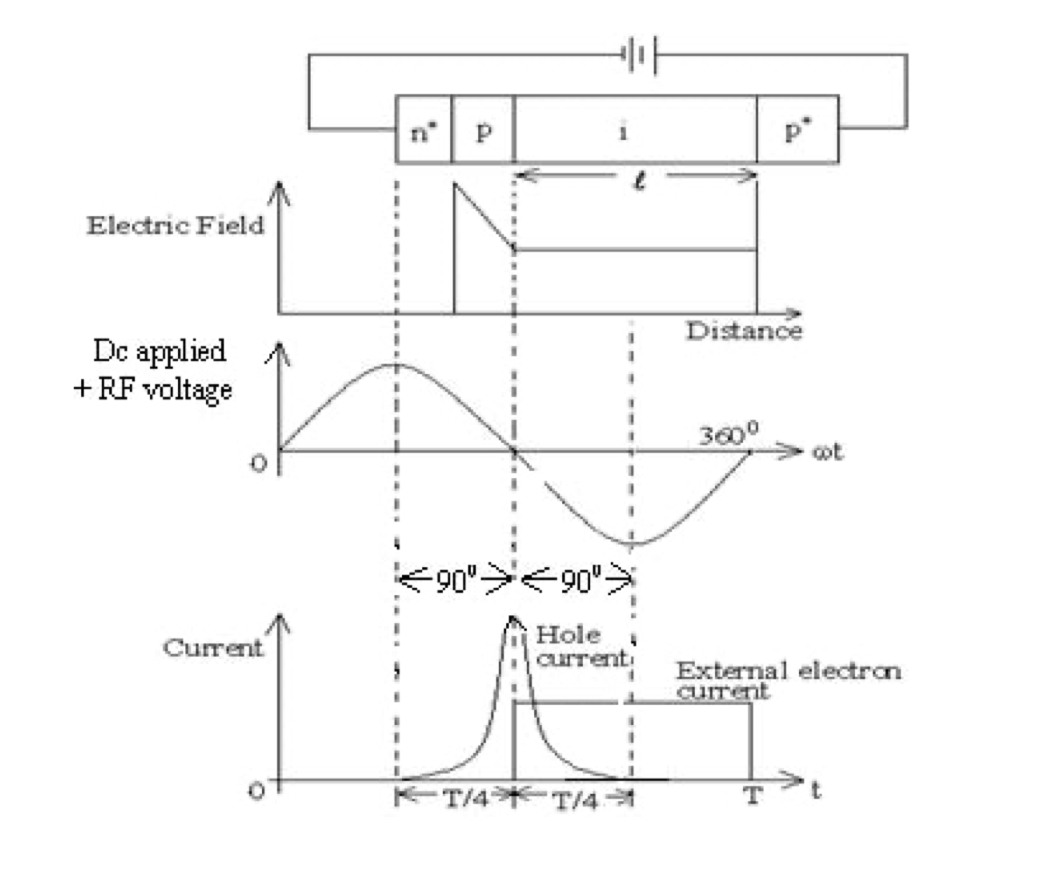
IMPATT Diode Theory
An IMPATT (Impact Avalanche Transit-Time) diode combines two regions:
- Avalanche Region → Reverse-biased beyond breakdown; carriers undergo impact ionization with multiplication factor M.
- Drift Region → Carriers traverse at near , introducing a phase delay between voltage and current.
The avalanche buildup time () and drift time () together set the oscillation frequency:
where drift time is given by:
The output RF power is given by:
where is the circuit efficiency.
Summary of Key Equations
| Equation | Expression | Description |
|---|---|---|
| (1) | Drift velocity | |
| (2) | Drift/diffusion transit time | |
| (3) | Tunneling probability | |
| (4) | Peak-to-valley current ratio | |
| (5) | IMPATT oscillation frequency |
These relationships form the theoretical basis for analyzing:
- High-speed carrier transport
- Negative-resistance switching
- Microwave generation in advanced semiconductor devices.