
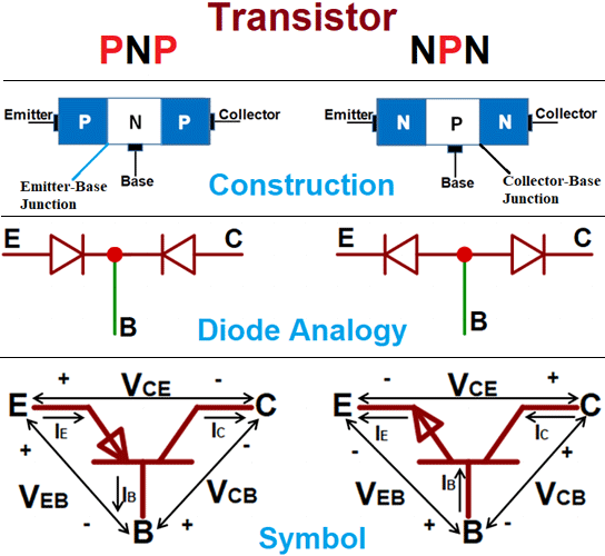
Bipolar Junction Transistors
Bipolar Junction Transistors (BJTs) are three-layer, two-junction semiconductor devices — either NPN or PNP — that can amplify or switch electrical signals.
They build directly on the physics of PN junctions, using two back-to-back junctions to control current flow.
Regions of a BJT:
- Emitter (E): Heavily doped to inject carriers efficiently.
- Base (B): Very thin and lightly doped to allow carriers to pass through with minimal recombination.
- Collector (C): Moderately doped and larger in area to collect carriers and dissipate heat.
3.2 Modes of Operation
The operation of a BJT depends on the biasing of its two PN junctions: the Emitter-Base (E-B) junction and the Collector-Base (C-B) junction.
| Mode | E-B Junction | C-B Junction | Characteristics |
|---|---|---|---|
| Cut-off | Reverse Biased | Reverse Biased | , transistor is OFF |
| Active (Forward) | Forward Biased | Reverse Biased | , used for amplification |
| Saturation | Forward Biased | Forward Biased | limited by circuit, transistor acts as closed switch |
| Reverse Active | Reverse Biased | Forward Biased | , reverse gain |
Detailed Operating Conditions:
Cut-off Mode:
- Both junctions are reverse-biased: (typically < 0.7 V for Si) and
- Voltage condition: The base voltage () is lower than both the collector voltage () and emitter voltage ()
- Collector current: (leakage current, typically nA range)
- Transistor acts as an open switch
Active Mode (Normal Operation):
- E-B junction forward-biased: V (Si), V (Ge)
- C-B junction reverse-biased: or equivalently
- Voltage condition: The base voltage () is higher than the emitter voltage () but lower than the collector voltage ()
- Collector current: where typically ranges from 50 to 300
- This mode is used for linear amplification
Saturation Mode:
- Both junctions forward-biased: and
- Voltage condition: The base voltage () is higher than both the emitter voltage () and collector voltage ()
- Collector-emitter voltage: V (Si)
- Current relationship no longer holds;
- Transistor acts as a closed switch in digital circuits
Reverse Active Mode:
- E-B junction reverse-biased and C-B junction forward-biased
- Rarely used; has poor characteristics with to (much less than )
- Emitter current:
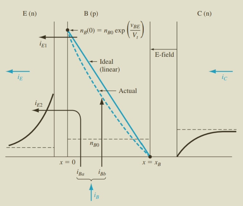
3.3 Carrier Transport in Active Mode
In active mode, the forward bias on the E-B junction injects majority carriers from the emitter into the base.
These carriers diffuse across the thin base and are swept into the collector by the reverse-biased C-B junction’s electric field.
Transport Mechanisms:
- Injection: High emitter doping → large carrier injection into the base.
- Diffusion: Carriers move through the base via diffusion due to a concentration gradient.
- Collection: Carriers reaching the base-collector junction are quickly swept into the collector.
3.4 Current Relationships
The fundamental relationship between the three terminal currents in a BJT is governed by Kirchhoff's Current Law:
where:
- = Emitter current (largest)
- = Collector current
- = Base current (smallest, typically 1-2% of )
3.4.1 Common-Base Current Gain ()
The common-base current gain (also called the base transport factor) is defined as:
For well-designed BJTs, , typically to .
The parameter can be further decomposed as:
where:
- = Emitter injection efficiency (fraction of emitter current due to majority carriers)
- = Base transport factor (fraction of injected carriers reaching collector)
- = Recombination factor accounting for carrier loss in base
3.4.2 Common-Emitter Current Gain ()
The common-emitter current gain (also called in hybrid parameters) is:
The relationship between and is derived from :
Solving for :
Conversely:
Typical values: ranges from 50 to 300 (sometimes up to 500 for high-gain transistors).
3.4.3 Active Mode Current Equations
In active mode, the collector current can be expressed as:
The emitter current:
Example: If , then:
If , then:
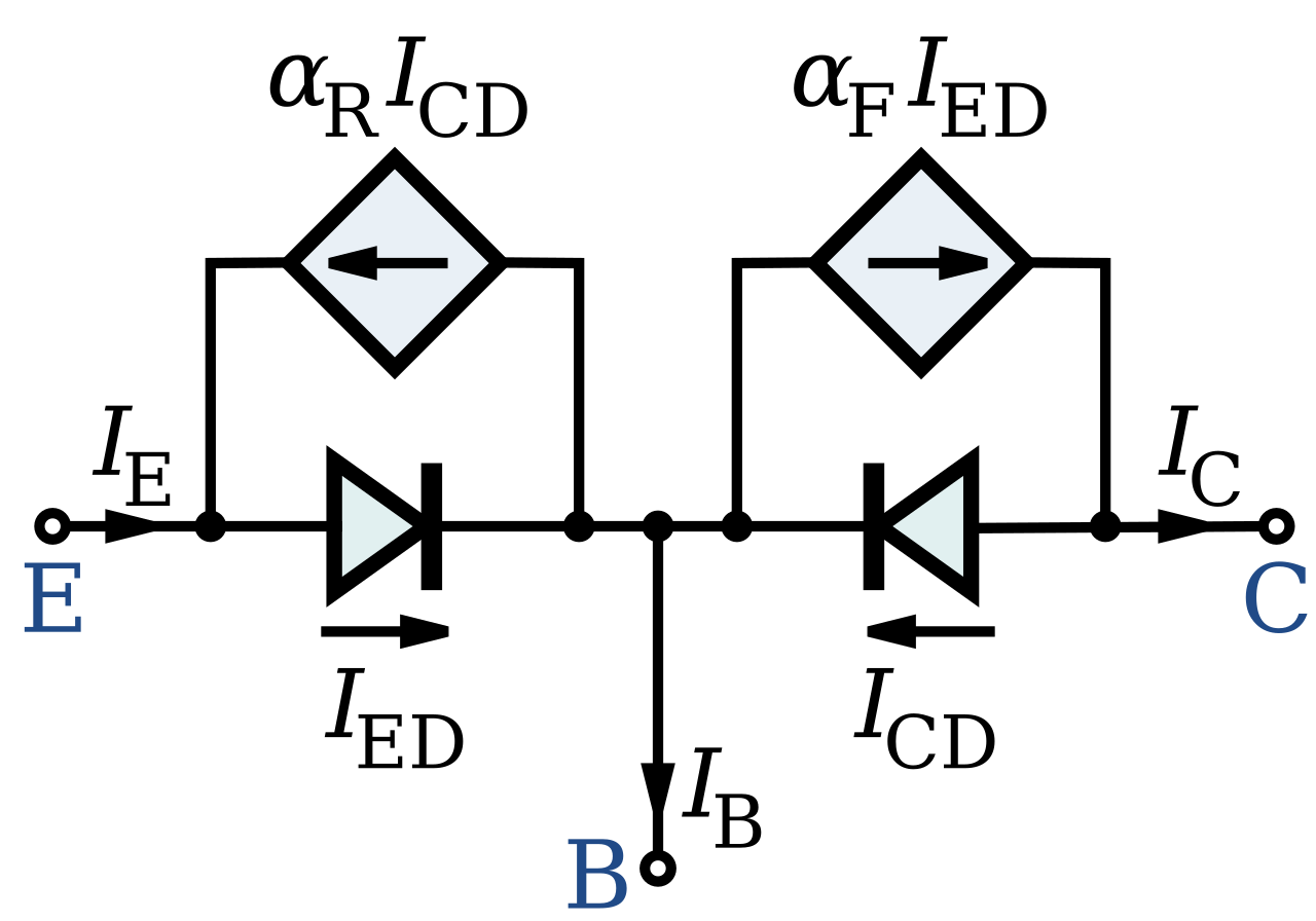
3.5 Ebers–Moll Model
The Ebers–Moll model describes a BJT in all regions of operation, using two coupled diodes.
Collector Current Equation:
Emitter Current Equation:
Where:
- = Saturation current of the transistor
- = Thermal voltage (~25.85 mV at room temperature)
- = Forward common-base gain
- = Reverse common-base gain
3.6 Configurations of BJT
A BJT can be connected in three basic configurations, each with different characteristics and applications. The choice of configuration depends on the desired gain characteristics, impedance levels, and application requirements.
3.6.1 Common-Emitter (CE) Configuration
In the Common-Emitter configuration, the input is applied between base-emitter and the output is taken between collector-emitter; the emitter is the common (grounded) terminal. This is the most widely used amplifier configuration because it provides both high current gain and high power gain.
Circuit Characteristics:
- Input: Base-Emitter (, )
- Output: Collector-Emitter (, )
- Common terminal: Emitter (grounded)
Current Relationships:
The emitter current relation is:
The current gain in CE configuration is:
where typically ranges from 20 to 200 for general-purpose BJTs.
Another important current ratio is:
with , usually around 0.95-0.99.
The relationship between and is:
Operating Principle:
A small change in base current causes a much larger change in collector current → this is the key amplification mechanism.
Key Parameters:
- Current gain: (high, typically 50-300)
- Voltage gain: (high, typically 100-500)
- Input impedance: (low to moderate, ~1-5 kΩ)
- Output impedance: (moderate, ~1-10 kΩ)
- Phase shift: 180° (inverting amplifier - input and output are out of phase)
Applications: Voltage amplifiers, power amplifiers, switching circuits
3.6.2 Common-Base (CB) Configuration
In the Common-Base configuration, the base terminal is common to both input and output; the input is applied between emitter and base, and output is taken between collector and base.
Circuit Characteristics:
- Input: Emitter-Base (, )
- Output: Collector-Base (, )
- Common terminal: Base (grounded)
Current Relationships:
The input current at the emitter is large, since:
Therefore, the collector current is slightly less than emitter current, giving:
This means the current gain is less than unity (unity or less).
Operating Principle:
Because the current gain is less than one, the CB amplifier attenuates current, not amplifies it. However, it is a non-inverting voltage amplifier → input and output voltages are in phase.
It has high voltage gain due to:
- Low input resistance (forward-biased emitter-base diode)
- High output resistance (reverse-biased collector-base junction)
Voltage Gain:
The Common-Base voltage gain is:
where is the load resistance and is the emitter resistance.
Resistance Gain:
The CB configuration exhibits significant resistance gain:
where is very low and is typically much larger.
Key Parameters:
- Current gain: (less than unity but close to 1)
- Voltage gain: (high, similar to CE)
- Input resistance: (very low, ~20-50 Ω)
- Output resistance: (very high, ~100 kΩ - 1 MΩ)
- Phase shift: 0° (non-inverting - input and output are in phase)
Applications: Not commonly used in general amplifiers, but useful in high-frequency applications due to low input capacitance and stable behavior; RF circuits, current buffers
3.6.3 Common-Collector (CC) Configuration (Emitter Follower)
In the Common-Collector configuration, the collector terminal is common to both input and output (usually tied to supply/ground through a resistor). The input signal is applied to the base, and the output is taken from the emitter, making it an Emitter Follower (output follows input).
Circuit Characteristics:
- Input: Base-Collector (, )
- Output: Emitter-Collector (, )
- Common terminal: Collector (usually connected to )
Current Relationships:
The load resistor is connected in series with the emitter, so the load current equals the emitter current.
Since:
the emitter current is larger than collector current, which leads to a high current gain.
Current Gain:
The current gain of the CC configuration is approximately:
which is much larger than of a CE amplifier.
Operating Principle:
It provides very high input impedance (hundreds of kΩ) and low output impedance, making it excellent for impedance matching.
The voltage gain is slightly less than 1, but the circuit provides no phase inversion, unlike CE configuration.
Key Parameters:
- Current gain: (high)
- Voltage gain: (unity, ~0.95-0.99)
- Input impedance: (very high, ~10-500 kΩ)
- Output impedance: (very low, ~10-100 Ω)
- Phase shift: 0° (non-inverting, output follows input)
Applications: Impedance matching circuits, buffer stages, voltage regulators, driver stages
Comparison Table:
| Parameter | Common-Emitter | Common-Base | Common-Collector |
|---|---|---|---|
| Current Gain | High () | Low () | High () |
| Voltage Gain | High (~100-500) | High (~100-500) | Unity (~1) |
| Power Gain | Very High | High | Medium |
| Input Impedance | Medium | Very Low | Very High |
| Output Impedance | Medium | Very High | Very Low |
| Phase Shift | 180° | 0° | 0° |
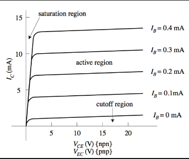
3.7 Output Characteristics
In the common-emitter configuration, the vs. characteristics exhibit distinct operating regions:
Characteristic Regions:
- Cut-off Region: , (leakage)
- Active Region: (nearly flat curves)
- Saturation Region: V, transistor fully ON
In the active region, the curves are nearly horizontal, indicating that:
- is primarily controlled by
- shows slight dependence on
The small positive slope in the active region is due to the Early Effect (also called base-width modulation).
3.7.1 Early Effect (Base-Width Modulation)
Definition: The Early Effect is the variation of the effective base width with changes in the collector-base reverse bias voltage. As increases, the depletion region at the collector-base junction widens, effectively reducing the neutral base width .
Physical Mechanism:
- Increasing (or ) increases the reverse bias on the C-B junction
- This widens the C-B depletion region, encroaching into the base
- The effective base width decreases:
- Carrier gradient in base increases: increases
- Collector current increases slightly
Mathematical Description:
The collector current including the Early Effect is:
where:
- = Early voltage (typically 50-200 V)
- = Saturation current
- = Thermal voltage ( mV at 300 K)
The output resistance in active mode is:
Practical Implications:
- Limits the maximum voltage gain of amplifiers
- Introduces finite output impedance ()
- Causes slight variation in with
- More pronounced in transistors with narrow base widths
Graphical Interpretation: When the - curves in the active region are extrapolated backward, they meet at a common point on the negative axis at voltage (the Early voltage).
3.8 Summary of Key Equations
Current Relationships:
Kirchhoff's Current Law:
Common-Base Current Gain:
Common-Emitter Current Gain:
Active-Mode Relationships:
Ebers-Moll Model:
Collector Current:
Emitter Current:
Active-Mode Approximations:
For and (reverse-biased C-B junction):
Including Early Effect:
where is the Early voltage.
Output Resistance:
Small-Signal Parameters:
Transconductance:
Input Resistance (Emitter Resistance):
Base-Emitter Input Resistance:
These equations are essential for designing amplifiers and switching circuits using BJTs.
References
For detailed derivations and additional information, refer to:
- S. M. Sze & K. Ng, Physics of Semiconductor Devices, Chapter 5: Bipolar Transistors
- B. G. Streetman & S. Banerjee, Solid State Electronic Devices, Chapter 6: BJTs
- R. F. Pierret, Advanced Semiconductor Fundamentals, Chapters 3-5
- Donald A. Neamen, Semiconductor Physics and Devices, Chapter 10: The Bipolar Transistor